Pete's Log: August Staycation, Day 1
Entry #1982, (Life in General, Smokepacking)(posted when I was 43 years old.)
I have some vacation to burn and also I've been feeling a little burned out and also also I had a few projects around the house I wanted to do get done, so a few weeks ago I put in a vacation request and now the time has come. My motivation level to work on those projects, however, has vanished. Two reasons:
- I still have a lingering tail end of my cold
- The world has conspired to make us no longer wish to host a party, making the house projects feel less urgent
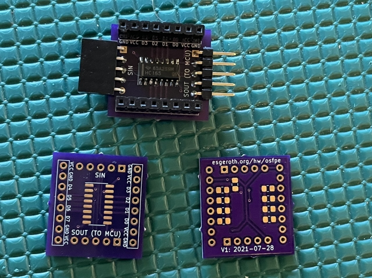
Sigh. But all is not lost. In the mail today, I received my second PCB design! Real nice of it to show up on a day that I have time to play with it.
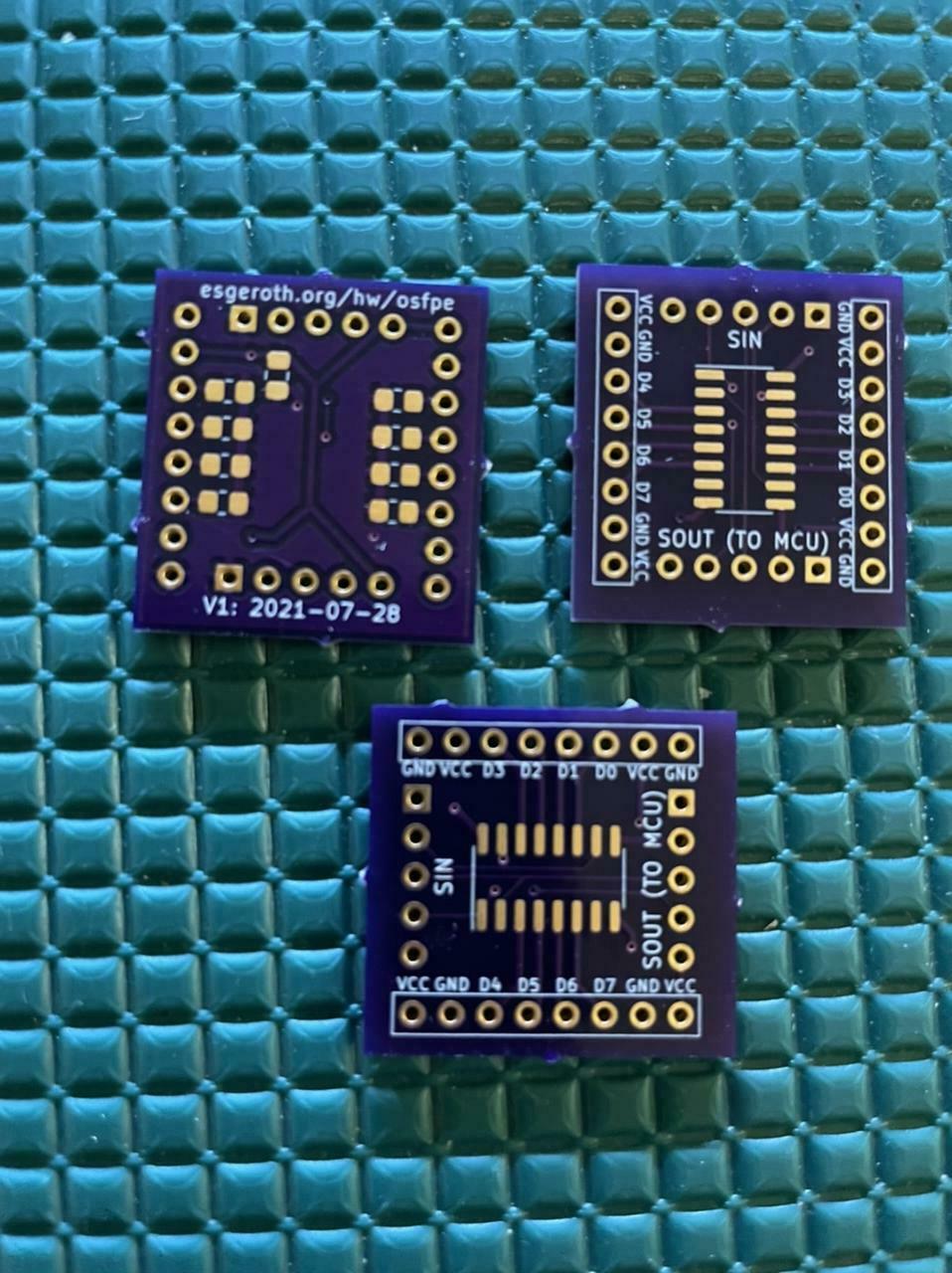
So let's do some bullets. I made this for a couple of reasons:
- As fun as the XOR Gate is, and as much as I did learn things making it, I felt like I needed more PCB design practice before attempting something more serious.
- Also, playing with KiCad is just fun.
- If I'm going to develop a 74HC165 component for ESPHome, I should have a variety of test platforms.
- I think I have a propensity to double down on absurdity.
So, in addition to owning at least 16 74HC165s in DIP16 format, I now also own 10 74HC165s in SOIC format. I paid $8 for them at digikey. Bringing the total cost of my 74HC165 habit above $20.
So here were my goals for this PCB:
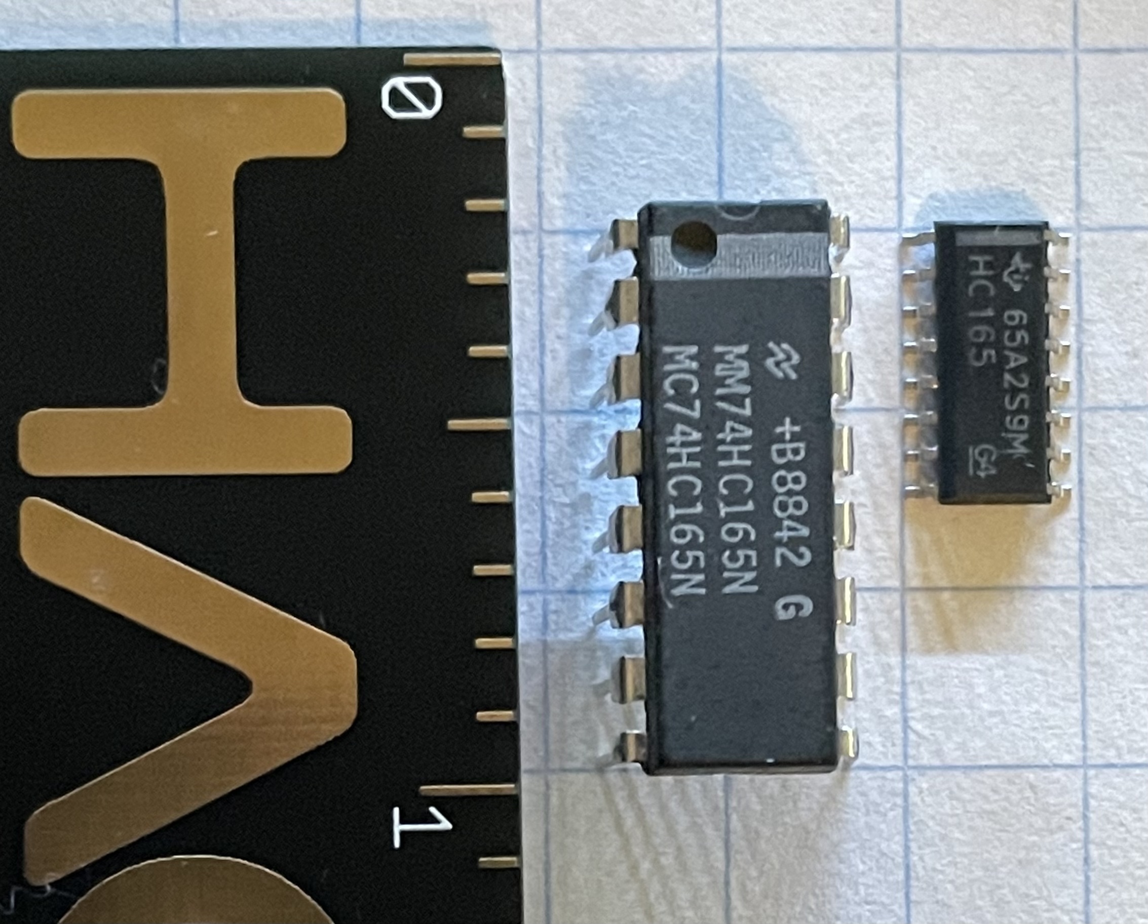
- Make it compact. This is one reason why I chose the SOIC package instead of using some of the DIP16 chips I already had, check this size comparison:
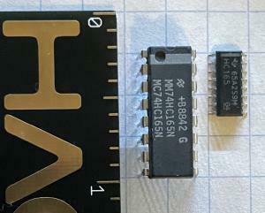
- Use components that are less forgiving than in the XOR Gate. In the XOR Gate if I got any size wrong, I could basically just bend the leads a bit to make up for it. I wanted footprints to really matter. So basically this meant using surface-mount components (the other reason I chose the SOIC package)
- Learn some new PCB things, like vias and copper pours
I think I succeeded on all my goals. The board itself is less than an inch square, meaning it cost less than $5 for three of them (and probably would've been even less if wasn't trying to get them American-made). That's including shipping, which still blows my mind.
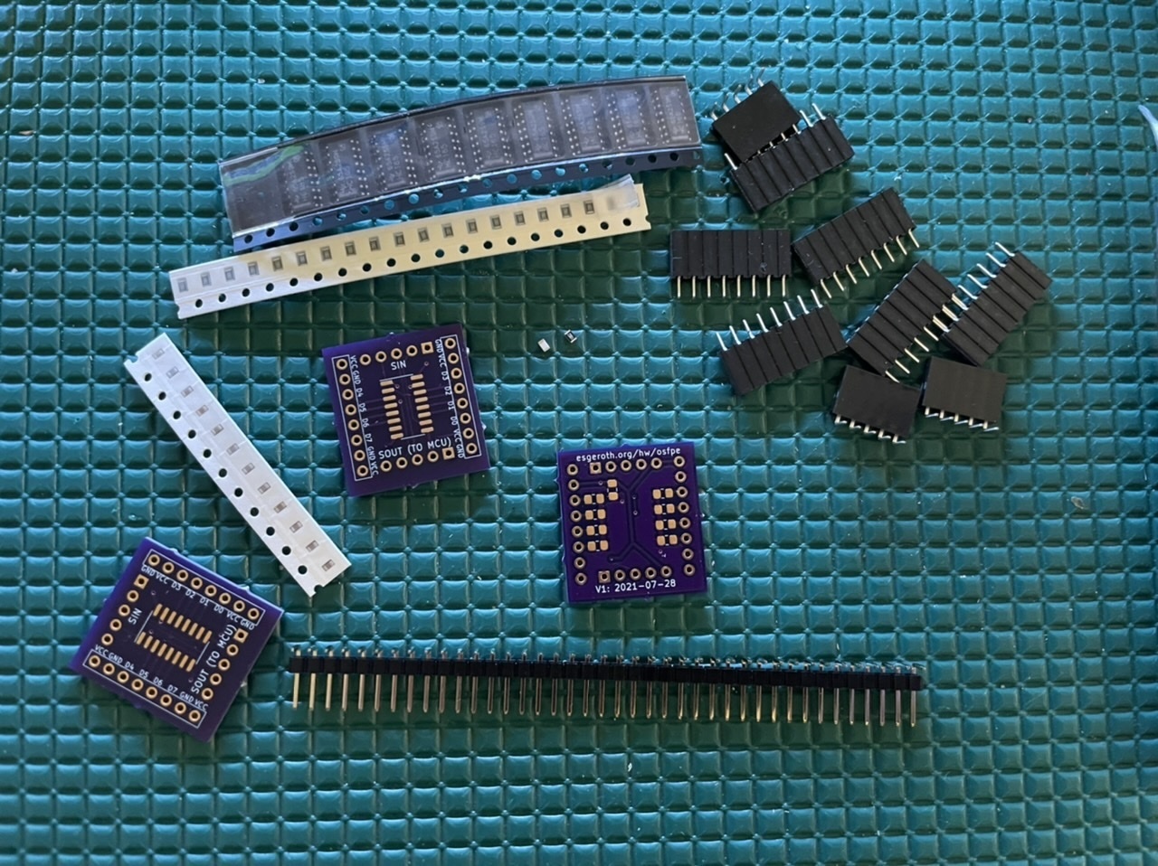
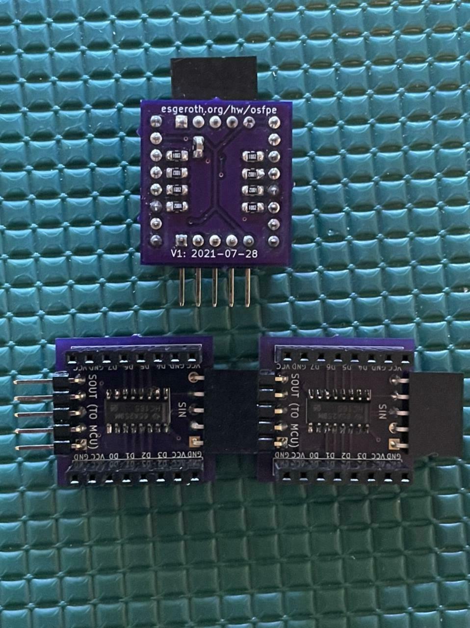
So time for some soldering.
One done, time to test. My debouncing tests had started to yield some fruit, so I tested this with a 555-based debouncing circuit. I didn't want to take my debouncing test apart, so this monstrosity was used for testing:

It works! Since unlike the XOR Gate I have reason to use more than one of these, let's assemble them all.
And give them a test. One thing I've come to realize is testing things with lots of inputs can get tedious. Three of these means 24 inputs. But here we go.
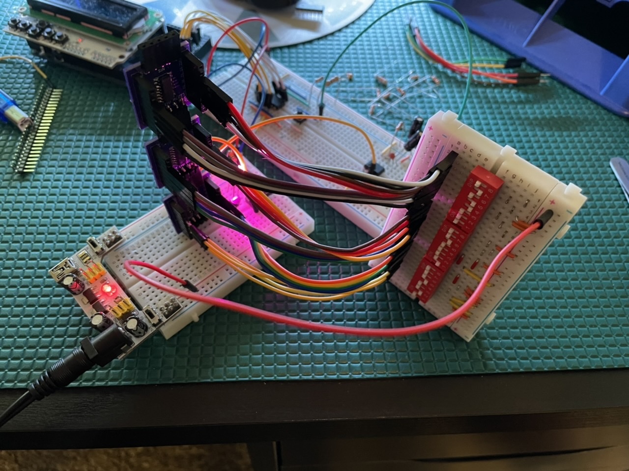
And it works!
Guess I have no excuses now to not write that 74HC165 component for ESPHome...